Difference between revisions of "Scratchpad unit"
(→Architecture) |
|||
| Line 25: | Line 25: | ||
===Architecture=== | ===Architecture=== | ||
[[File:SPM_arch.png|center|thumb|High-level SPM architectural view]] | [[File:SPM_arch.png|center|thumb|High-level SPM architectural view]] | ||
| + | The Address Mapping Unit computes in parallel the bank index and the bank offset for each of the L memory addresses coming from the processor lanes. Bank index (BI i in figure abpve) is the index of the bank to which the address is mapped. Bank offset (BO i in figure above) is the address of the word into the bank. The Address Mapping Unit behaviour can be changed at run time in order to change the relationship between addresses and banks. This is a key feature in that it allows the adoption of the mapping strategy that best suits the executed workload. The Serialization Logic Unit performs the conflict detection and the serialization of the conflicting requests. Whenever an n-way conflict is detected, the Serialization Logic Unit puts the SPM in the busy state and splits the requests into n conflict-free requests issued serially in the next n clock cycles. When the last request is issued, the Serialization Logic Unit put the SPM in the ready state. Notice that for the Serialization Logic Unit, multiple accesses to the same address are not seen as a conflict, as in this occurrence a broadcast mechanism is activated. This broadcast mechanism provides an efficient way to satisfy multiple load requests for the same constant parameters. The Input Interconnect is an interconnection network that steers source data and/or control signals coming from a lane in the GPU-like processor to the destination bank. Because the Input Interconnect follows the Serialization Logic Unit, it only accepts one request per bank. Then, there are the B memory banks providing the required memory elements. Each memory bank receives the bank offset, the source data, and the control signal form the lane that addressed it. Each bank has a single read/write port with a byte-level write enable signal to support instructions with operand sizes smaller than word. Furthermore, each lane controls a bit in an L-bit mask bus that is propagated through the Input Interconnect to the appropriate bank. This bit acts as a bank enable signal. In this way, we can disable some lanes and execute operations on a vector smaller than L elements. The Output Interconnect propagates the loaded data to the lane that requested it. Last, there is a Collector Unit which is a set of L registers that collect the | ||
| + | results coming from the serialized requests outputting them as a single vector. | ||
| + | |||
===Customizable features=== | ===Customizable features=== | ||
Revision as of 17:55, 4 May 2019
Like existing GPU-like core projects, nu+ provides limited hardware support for shared scratchpad memory. The nu+ core presents a configurable GPU-like oriented scratchpad memory (SPM) with built-in support for bank remapping. Typically, scratchpad memories are organized in multiple independently-accessible memory banks. Therefore if all memory accesses request data mapped to different banks, they can be handled in parallel (at best, with L memory banks, L different gather/scatter fulfilled in one clock cycle). Bank conflicts occur whenever multiple requests are made for data within the same bank. If N parallel memory accesses request the same bank, the hardware serializes the memory accesses, causing an N-way conflict and an N-times slowdown. The nu+ SPM dynamic bank remapping mechanism, based on specific kernel access pattern, minimizes bank conflicts.
Contents
Interface and operation
Interface
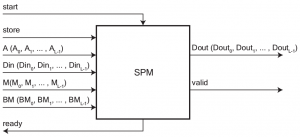
As shown in the figure above, the I/O interface of the SPM has several control and data signals. Due to the scattered memory access of the processor, all the data signals, both in input and in output, are vectors and every index identifies a corresponding lane of the core unit. So, SPM has the following data inputs for each lane:
A: address of the memory location to be accessed;Din: word containing data to be written (in the case of scatter operation);BM[0..W-1]: W-bit-long bitmask to enable/disable the writing of each byte ofDinword;M: bit asserted if the lane will participate in the next instruction execution.
As for inputs, the SPM has a single data output for each lane that is:
Dout: data stored at the addresses contained inA.
The store signal is an input control signal. If store is high, the requested instruction will be a scatter operation, otherwise it is a gather one. The value of store signal is the same for all the lanes. Due to the variability of latency it is necessary to introduce some control signals that allow to implement a handshaking protocol between the control logic of the SIMD core (owner of the CUDA Thread Block) and the SPM control logic. These signals are:
startis an input signal and is asserted by the core control unit to request the execution of an instruction;readyis an output signal and is asserted by the SPM when it can process a new instruction;validis an output signal and is asserted by the SPM when the execution of an instruction is finished and its outputs are the final outcome.
FSM model
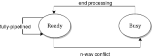
As said, the SPM takes as input L different addresses to provide support to the scattered memory access (and its multi-banking implementation). It can be regarded as a finite state machine with the following two states:
- Ready
- - the SPM is ready to accept a new memory request.
- Busy
- - the SPM cannot accept any request as it is still processing the previous one.
In the Ready state the ready signal is high. In the Busy state all input requests will be ignored. Assuming the loaded instruction relates to conflicting addresses, the SPM goes into the Busy state and sets the ready signal as low. At the end of the memory access serialization, the SPM passes into the Ready state. If the SPM is involved in the execution of another instruction, the ready signal is low and the input instruction is not yet accepted. If an instruction is free of conflicts, the SPM executes it without passing in the Busy state. So consecutive instructions without conflicts can be executed without interruptions, just as if the SPM were a fully pipelined execution unit.
Architecture
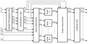
The Address Mapping Unit computes in parallel the bank index and the bank offset for each of the L memory addresses coming from the processor lanes. Bank index (BI i in figure abpve) is the index of the bank to which the address is mapped. Bank offset (BO i in figure above) is the address of the word into the bank. The Address Mapping Unit behaviour can be changed at run time in order to change the relationship between addresses and banks. This is a key feature in that it allows the adoption of the mapping strategy that best suits the executed workload. The Serialization Logic Unit performs the conflict detection and the serialization of the conflicting requests. Whenever an n-way conflict is detected, the Serialization Logic Unit puts the SPM in the busy state and splits the requests into n conflict-free requests issued serially in the next n clock cycles. When the last request is issued, the Serialization Logic Unit put the SPM in the ready state. Notice that for the Serialization Logic Unit, multiple accesses to the same address are not seen as a conflict, as in this occurrence a broadcast mechanism is activated. This broadcast mechanism provides an efficient way to satisfy multiple load requests for the same constant parameters. The Input Interconnect is an interconnection network that steers source data and/or control signals coming from a lane in the GPU-like processor to the destination bank. Because the Input Interconnect follows the Serialization Logic Unit, it only accepts one request per bank. Then, there are the B memory banks providing the required memory elements. Each memory bank receives the bank offset, the source data, and the control signal form the lane that addressed it. Each bank has a single read/write port with a byte-level write enable signal to support instructions with operand sizes smaller than word. Furthermore, each lane controls a bit in an L-bit mask bus that is propagated through the Input Interconnect to the appropriate bank. This bit acts as a bank enable signal. In this way, we can disable some lanes and execute operations on a vector smaller than L elements. The Output Interconnect propagates the loaded data to the lane that requested it. Last, there is a Collector Unit which is a set of L registers that collect the results coming from the serialized requests outputting them as a single vector.
Customizable features
2/5/2019
INTERFACCIA E FUNZIONALITA'
Vista modulare con ingressi-uscite (con descrizione)
24/4/2019
INTERFACCIA E FUNZIONALITA'
Vista modulare con ingressi-uscite (con descrizione) FSM (differenza comportamento fully-pipelined e n-way conflicts) ingressi parametrizzabili
MODULI
Stadio 0 (pipe) Stadio 1 (stage1) Stadio 2 (stage2) Stadio 3 (stage3)
ESEMPIO DI FUNZIONAMENTO
Si deve aggiungere l'attributo __scratchpad per avere la sicurezza che una variabile venga allocata in SPM. Definire qualche esempio più specifico (e.g. conv_layer_mvect_mt con uno o due core)


