Scratchpad unit
The NaplesPU core presents a configurable GPU-like oriented scratchpad memory (SPM) with built-in support for bank remapping. Typically, scratchpad memories are organized in multiple independently-accessible memory banks. Therefore if all memory accesses request data mapped to different banks, they can be handled in parallel (at best, with L memory banks, L different gather/scatter fulfilled in one clock cycle). Bank conflicts occur whenever multiple requests are made for data within the same bank. If N parallel memory accesses request the same bank, the hardware serializes the memory accesses, causing an N-way conflict and an N-times slowdown. The NaplesPU SPM dynamic bank remapping mechanism, based on specific kernel access pattern, minimizes bank conflicts.
Interface and operation
Interface
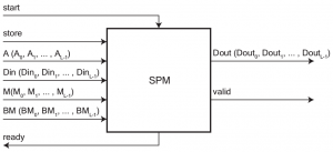
As shown in the figure above, the I/O interface of the SPM has control and data signals. Due to the scattered memory access of the processor, all the data signals, both in input and in output, are vectors and every index identifies a corresponding lane of the core unit. So, SPM has the following data inputs for each lane:
A: address of the memory location to be accessed;Din: word containing data to be written (in the case of scatter operation);BM[0..W-1]: W-bit-long bitmask to enable/disable the writing of each byte ofDinword;M: bit asserted if the lane will participate in the next instruction execution.
As for inputs, the SPM has a single data output for each lane that is:
Dout: data stored at the addresses contained inA.
The store signal is an input control signal. If store is high, the requested instruction will be a scatter operation, otherwise it is a gather one. The value of the store signal is the same for all the lanes. Due to the variability of latency, it is necessary to introduce some control signals that allow implementing a handshaking protocol between the control logic of the SIMD core and the SPM control logic. These signals are:
startis an input signal and is asserted by the core control unit to request the execution of an instruction;readyis an output signal and is asserted by the SPM when can process a new instruction;validis an output signal and is asserted by the SPM when the execution of an instruction is finished and its outputs are the final outcome.
FSM model
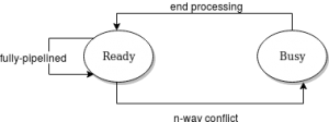
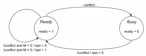
As said, the SPM takes as input L different addresses to provide support to the scattered memory access (and its multi-banking implementation). It can be regarded as a finite state machine with the following two states:
- Ready
- - the SPM is ready to accept a new memory request.
- Busy
- - the SPM cannot accept any request as it is still processing the previous one.
In the Ready state the ready signal is high and there are no issuing requests. In the Busy state all input requests will be ignored. Assuming the loaded instruction relates to conflicting addresses, the SPM goes into the Busy state and sets the ready signal as low. At the end of the memory access serialization, the SPM passes into the Ready state. If the SPM is involved in the execution of another instruction, the ready signal is low and the input instruction is not yet accepted. If an instruction is free of conflicts, the SPM executes it without passing in the Busy state. So consecutive instructions without conflicts can be executed without interruptions, just as if the SPM were a fully pipelined execution unit.
Customizable features
The SPM is totally configurable. In particular it is possible to customize the number of lanes of the SIMD core unit (L), the number of memory banks (B), the number of entries contained in a bank (D) and the number of bytes that make up an entry in a memory bank (W) simply by changing the value of the respective parameters in the SPM configuration file.
`define SM_PROCESSING_ELEMENTS      16		//L
`define SM_ENTRIES                  1024	//D
`define SM_MEMORY_BANKS             16		//B
`define SM_BYTE_PER_ENTRY           4		//W
`define SM_ENTRY_ADDRESS_LEN        $clog2(`SM_ENTRIES) 	//entry address lenght
`define SM_MEMORY_BANK_ADDRESS_LEN  $clog2(`SM_MEMORY_BANKS) 	//memory bank address lenght
`define SM_BYTE_ADDRESS_LEN         $clog2(`SM_BYTE_PER_ENTRY) 	//byte address lenght
`define SM_ADDRESS_LEN              `SM_ENTRY_ADDRESS_LEN + `SM_MEMORY_BANK_ADDRESS_LEN + `SM_BYTE_ADDRESS_LEN 	//address length
The overall size of the SPM is given by B*D*W/8 bit.
Architecture
Overview
The scratchpad unit is composed of the scratchpad memory and a FIFO request queue. The unit receives inputs from operand fetch unit and outputs toward the rollback unit and the writeback unit. The FIFO request queue size is customizable. A general request enqueued and forwarded to the SPM is organized as follows:
typedef struct packed {
	logic 	 							is_store;
	sm_address_t 	[`SM_PROCESSING_ELEMENTS   - 1 : 0] 		addresses;
	sm_data_t 	[`SM_PROCESSING_ELEMENTS      - 1 : 0] 		write_data;
	sm_byte_mask_t 	[`SM_PROCESSING_ELEMENTS - 1 : 0] 		byte_mask;
	logic 		[`SM_PROCESSING_ELEMENTS          - 1 : 0] 	mask;
	logic 		[`SM_PIGGYBACK_DATA_LEN           - 1 : 0] 	piggyback_data;
} scratchpad_memory_request_t;
Before the requests are queued, a phase of decoding and alignment checking of the type of operation and bitmask generation based on the opcode (to determine which lane are involved) is performed. Afterwards the control logic checks the alignment of the incoming request. Supported operations are both scalar and vector and on byte, half-word and word-aligned addresses. The alignment is checked by the following coding lines:
assign is_word_aligned		[lane_idx]	= !( |( effective_addresses[lane_idx][1 : 0] ) );
assign is_halfword_aligned	[lane_idx]	= !effective_addresses[lane_idx][0];
Then, the following code determines if the access is misaligned based on the current operation, the required alignment for the memory access and the lane mask:
assign is_misaligned = ( is_word_op	 && ( |( ~is_word_aligned	& mask[`HW_LANE - 1 : 0] ) ) ) ||
			( is_halfword_op && ( |( ~is_halfword_aligned	& mask[`HW_LANE - 1 : 0] ) ) );
In case of misaligned access or out-of-memory address, the unit enables the Rollback handler, which launches the corresponding trap.
always_ff @ ( posedge clk, posedge reset )
	if ( reset )
		spm_rollback_en <= 1'b0;
	else
		spm_rollback_en <= instruction_valid & ( is_misaligned | is_out_of_memory ); //Rollback handler enabled

always_ff @ ( posedge clk ) begin
	spm_rollback_pc        <= `SPM_ADDR_MISALIGN_ISR; //location of the corresponding trap
	spm_rollback_thread_id <= opf_inst_scheduled.thread_id;
end
If an instruction is aligned, a new scratchpad_memory_request_t instance is created and filled accordly aligned with the operation type. Then, the new request is enqueued in the FIFO request queue, but only if the instruction is valid and if there is no rollback occurring. When the SPM is in the Ready state (the ready signal is high) and the FIFO queue is not empty, the oldest request is dequeued and comes to the SPM. At the end of the SPM execution (when the valid signal is high), the last phase aims to output the results. In case of conflicting operations, results will be available only at the end of all the serialized requests.
Stage 1
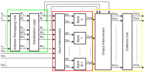
The first stage (in the green box in the figure above) has the task of carrying out conflict detection and serialization of conflicting memory requests. If the SPM is in the Ready state, it will carry out the incoming requests. If a conflict is detected while the SPM is in the Ready state, the SPM moves to the Busy state and serializes conflicting requests. If the SPM is in the Busy state, it will not accept inputs until the last serialized requests is served.
Address Remapping Unit
The Address Remapping Unit computes in parallel the bank index and the bank offset for each of the L memory addresses coming from the processor lanes. Bank index (BI[0..L-1] in figure above) is the index of the bank to which the address is mapped. Bank offset (BO[0..L-1] in figure above) is the displacement of the word into the bank. Furthermore, the Address Remapping Unit behavior can be changed at runtime in order to change the relationship between addresses and banks, allowing the adoption of the mapping strategy that best suits the executed workload. The Address Decode Unit is the component dedicated to actually performing the decoding process of the mapping strategy. The cyclic-mapping strategy is the only currently supported and is very easy to implement: it assigns the first word to the first memory bank, the second word to the second memory bank and so on, repeating the assignment process every B times (where B is the number of memory banks) and considering bank indexes 0 and B-1 as consecutive. For the cyclic-mapping strategy, indexes e offsets are obtained simply dividing the address as follows.
assign bank_offset    = address[`SM_ADDRESS_LEN - 1   -:  `SM_ENTRY_ADDRESS_LEN        ];
assign bank_index     = address[`SM_BYTE_ADDRESS_LEN  +:  `SM_MEMORY_BANK_ADDRESS_LEN  ];
Serialization Logic Unit
The Serialization Logic Unit performs the conflict detection and the serialization of the conflicting requests. It implements an iterative algorithm which defines a set of non-conflicting pending requests to be executed at every clock cycle. Whenever an n-way conflict is detected, the Serialization Logic Unit puts the SPM in the Busy state and splits the requests into n conflict-free requests issued serially in the next n clock cycles, causing an n-times slowdown. When the last request is issued, the Serialization Logic Unit put the SPM in the Ready state. Notice that for the Serialization Logic Unit, multiple accesses to the same address are not seen as a conflict, as in this occurrence a broadcast mechanism is activated. This broadcast mechanism provides an efficient way to satisfy multiple read requests for the same word.
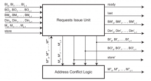
Among other things, as shown in the figure above, the Serialization Logic Unit takes in input the L-bit-long mask (M in the figure above) identifying the lanes to serve. At every clock cycle, it keeps track of the requests to be served in that cycle and to postpone to the next cycle by defining three masks of L bits:
M': pending requests' mask;M'': mask of non-conflicting pending requests to serve in the current clock cycle;M''': mask of still-conflicting pending requests to postpone.
The Serialization Logic Unit is composed of two main components: the Request Issue Unit and the Address Conflict Logic.
Request Issue Unit
The Request Issue Unit has the task of storing information about requests throughout the serialization process.
The Requests Issue Unit keeps the information on a set of requests for as long as it takes to satisfy it, saving the information in a set of internal registers. When the unit is in the Ready state, it selects the bitmask received from the SPM (M in the figure above or input_pending_mask in the snippet below) as pending requests' mask (M') and saves the datapath internally. When the unit is in the Busy state, it rejects input mask from SPM, internal registers are disabled and a multiplexer outputs data previously saved in internal registers. The unit remains in the Busy state and uses the still-conflicting pending requests' mask (M''') received from the Address Conflict Logic as pending requests' mask (M') until it receives a completely-low bitmask and the serialization process comes to an end. The following code shows the output decoder based on the current state of the unit:
always_comb begin
	case (current_state)
		READY :
		begin
			output_selection        = 1'b0;
			input_reg_enable        = 1'b1;
			ready                   = 1'b1;
			output_is_last_request  = !conflict && (|input_pending_mask != 0);
		end
		ISSUING_REQUESTS :
		begin
			output_selection        = 1'b1;
			input_reg_enable        = 1'b0;
			ready                   = 1'b0;
			output_is_last_request  = !conflict;
		end
	endcase
end
The unit moves to the Busy state whenever it detects a conflict.
assign conflict = (|input_still_pending_mask != 0);
The last signal is asserted when a whole set of requests from an instruction is satisfied in a clock cycle. This signal will be used by the Collector Unit to validate the collection of the results of a block of serialized requests.
Address Conflict Logic
The Address Conflict Logic analyzes the mask of pending requests and determines a subset of non-conflicting requests that can be satisfied in the current clock cycle. Still-conflicting requests are defined doing a bitwise and between the pending requests' mask and the 1's complement of requests satisfied during the current clock cycle. Then, they are sent back to the Request Issue Unit according to the following code:
assign still_pending_mask = ~satisfied_mask & pending_mask;
The unit gives a priority value to each request and selects the highest priority request and the set of pending requests which do not point to the same memory bank as the set that can be executed. The priority value is related to the lane index (requests from lane 0 have the highest priority value and so on) and the evaluation takes up just one clock cycle. The Address Conflict Logic is composed of the following parts:
- Conflict Detection: it makes the conflicting requests' mask by comparing bank indexes of pending requests. If a request is pending and collides with an higher-priority request, the conflicts' mask will set a high bit in the position of the lower-priority lane. It is worth noting that all comparators are in parallel.
generate
	for (i = 0; i < `SM_PROCESSING_ELEMENTS; i++) begin
		for (j = i + 1; j < `SM_PROCESSING_ELEMENTS; j++)
			assign conflict_matrix[j][i] = ((bank_offsets[i] == bank_offsets[j]) && pending_mask[i]);
	end
endgenerate
- Broadcast Selection: it implements the broadcasting mechanism, useful if several lanes require the read operation on the same word. It elects the address of the higher-priority pending request as broadcast address. Then it compares the bank indexes and the bank offsets of the pending requests with those of the elected broadcast address and sets a high bit in the position of the lane that refers to the same address. Since broadcasting makes sense for read-only instructions, the comparators' outputs are put in an AND gate together with the
¬store(surely high due to the read operation) to generate the broadcast mask.
generate
	for (i = 0; i < `SM_PROCESSING_ELEMENTS; i++)
		assign broadcast_mask[i] = ((bank_indexes[i] == broadcast_bank_index) && (bank_offsets[i] == broadcast_bank_offset)
						&& !is_store);
endgenerate
- Decision Logic: it determines the mask of the requests to be processed in the current clock cycle, starting from the conflicts' mask and the broadcast mask. A request can be executed immediately only if does not collide with any higher-priority request or if wants to read from the broadcast address. The useful requests are set according to the following code:
generate
	for (i = 0; i < `SM_PROCESSING_ELEMENTS; i++)
		assign satisfied_mask[i] = pending_mask[i] && (broadcast_mask[i] || !conflicts_mask[i]);
endgenerate
Stage 2
The second stage (in the red box in the figure above) hosts the memory banks. According to the address, incoming requests from the lanes are forwarded to the appropriate memory bank.
Input Interconnect
The Input Interconnect is an interconnection network that steers source data and/or control signals coming from a lane of the core to the destination bank. Because the Input Interconnect follows the Serialization Logic Unit, it only accepts one request per bank. Its structure is composed of as many Bank Steering Units as there are memory banks.
Bank Steering Unit
Each Bank Steering Unit selects any request that refers to the i-th memory bank among all requests to be processed and forwards it correctly. A set of L comparators firstly checks if the bank indexes and the preloaded index i are equal. Then the results are forwarded to an AND gate together with the mask of the requests to be processed in the current clock cycle. In the case of read operations, due to the broadcasting mechanism, the bank offsets of incoming requests are all the same, so requests are equivalent and it is possible to forward any of them to the memory bank. The bitmask of pending requests of the i-th memory bank are sent to the Priority Encoder that chooses the index of the highest-priority pending request. To avoid performing incorrect operations, if there is no request for the selected memory bank, the selected index is put in an AND gate with the validity output of the Priority Encoder. Therefore, this output is high only if there is actually a request to be processed for the i-th memory bank.
generate
	for (i = 0; i < `SM_PROCESSING_ELEMENTS; i++)
		assign compare_mask[i] = input_bank_indexes[i] == BANK_ADDRESS;
endgenerate

priority_encoder_npu #(
	.INPUT_WIDTH(`SM_PROCESSING_ELEMENTS),
	.MAX_PRIORITY("LSB")
) controller (
	.decode(input_mask & compare_mask), //input_mask is satisfied_mask from Input Interconnect
	.encode(selected_address),
	.valid(priority_encoder_valid)
);

assign output_enable = input_mask[selected_address] & priority_encoder_valid;
Banked memory
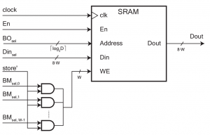
The storage unit is partitioned into B memory banks. Each memory bank receives the bank offset, the source data, and the control signal form the lane that addressed it. It is a read-first SRAM module: if a write operation occurs, the memory bank firstly will output the content located at the selected address and then it will overwrite it. Each memory bank has a single read/write port with a byte-level write enable signal to support instructions with operand sizes smaller than word (WE in the figure below). Furthermore, each lane controls a bit in an L-bit mask bus that is propagated through the Input Interconnect to the appropriate bank and this bit acts as a memory bank enable signal (En in the figure below).
Stage 3
The third and final stage (in the yellow box in the figure above) propagates the data output from the memory banks to the lanes that request it storing the result in the corresponding register. If any conflicting requests have been serialized and the last signal coming in input from the Serialization Logic is high, results will be validated (setting the valid output of the SPM as high) and sent out as a single vector. Due to the memory banks' latency, the non-conflicting requests' mask and the last signal are delayed to make sure that they come alongside the data linked to the corresponding request.
Output Interconnect
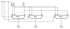
The Output Interconnect propagates data to the lane that requested it. As shown in the figure below, it is composed of a set of L multiplexer which interconnects all the memory banks with all lanes. Each multiplexer selects one among memory banks' outputs based on the value of the bank index received from the Serialization Logic and sends it toward the lane from which were addressed. If several lanes require the same data, the requests' bank indexes will be the same and therefore multiplexers will forward the same data to different lanes (according to the broadcasting).
Collector Unit
At the end of the pipe there is a Collector Unit which is a set of L registers that collect the results coming from the serialized requests outputting them as a single vector. It saves the results received from the Output Interconnection in a series of L registers. Each register is enabled by the corresponding bit of the mask of non-conflicting requests to be satisfied in the current clock cycle outgoing from the Serialization Logic. When a request is served successfully, its result is stored in the paired register as shown in the following code.
genvar lane_idx;
generate
	for (lane_idx = 0; lane_idx < `SM_PROCESSING_ELEMENTS; lane_idx++) begin
		always_ff @(posedge clock, negedge resetn) begin
			if (!resetn) begin
				//reset
			end else begin
				if (sm2_satisfied_mask[lane_idx])
					sm3_read_data[lane_idx] <= ii_output_data[lane_idx];
				end
			end
		end
endgenerate
Usage example
As said above, usage of scratchpad memory must be explicitly defined by programmers.
To specify that a variable must be saved in the SPM, the global scope and the __scratchpad attribute in the declaration line of the variable are mandatory.
Assembly output
So, we can declare a variable using the SPM attibute as follows:
__scratchpad int test_counter = 0;
Then, the NaplesPU compiler saves it in the corresponding memory area during the execution startup rutines (crt0). Before the execution of the main function, a portion of available memory address space equal to the SPM size is dynamically instantiated and data and variables defined with the SPM attribute are mapped into. In the object file, the SPM initialization is identified by preload_scratchpad, preload_scratchpad_vector, preload_scratchpad_words, preload_scratchpad_remain_bytes labels.
Analyzing the object file made by the compiler, it is easy to recognize parts of SPM-based instructions in the source code.
For instance, the following C++ code line
test_counter += 10;
is translated after compilation as the following assembly lines, according to the ISA.
5e8:	02 00 04 82 	load32_scratchpad s1, (s0)
5ec:	50 10 04 44 	addi s1, s1, 10
5f0:	02 00 04 a2 	store32_scratchpad s1, (s0)
Kernel example: matrix multiplication
The use of SPM is illustrated through the example of a matrix multiplication C = A*B with A, B and C of NxN dimensions.
In the header file, macros and global variables are defined as follows:
 #define TILE_DIM THREAD_NUMB
 __scratchpad int As[TILE_DIM][N];
 __scratchpad int Bs[N][TILE_DIM];
Moreover, the following code is an example of tiled matrix multiplication kernel.
 void mmsc_tiling (int C[N][N], const int A[N][N], const int B[N][N]) {
   for (unsigned turn = 0; turn < N / TILE_DIM; turn++) {
     unsigned int col0 = turn * TILE_DIM; //starting column for the current tile
     unsigned int tid = THREAD_ID;
     unsigned int row = CORE_ID * TILE_DIM + tid; //row index assigned to the given thread

     // NxTILE_DIM sub-matrix of B from global to scratchpad memory
     if (THREAD_ID == 0)
       for (unsigned int i = 0; i < N; i++)
         for (unsigned int j = 0; j < TILE_DIM; j++)
           Bs[i][j] = B[i][col0 + j];

     __builtin_npu_barrier(CORE_ID + 1, THREAD_NUMB - 1);

     // row of input matrix A from global to scratchpad memory
     for (unsigned int i = 0; i < N; i++)
       As[tid][i] = A[row][i];

     int sum = 0;
     for (unsigned int col = 0; col < TILE_DIM; col++) {
       sum = 0;

       // evaluation of single element of C matrix
       for (unsigned int i = 0; i < N; i++)
         sum += As[tid][i] * Bs[i][col];

       // last evaluated element of C from scratchpad to global memory
       C[row][col + col0] = sum;
     }
   }
 }
The matrix multiplication is divided into N/TILE_DIM iterations. Within each iteration of the outer for loop, every thread computes
TILE_DIM elements of the output matrix C and every core evaluates the multiplication between a TILE_DIMxN sub-matrix of A and a NxTILE_DIM sub-matrix of B. The As and Bs sub-matrices are stored into the local scratchpad memory, saving memory transactions since data from main memory are fetched only once per iteration. To keep the kernel simple, TILE_DIM must be equal to N / CORE_NUMB (where CORE_NUMB is the number of running cores). Furthermore, the total number of running cores and threads must be equal to the following formula: CORE_NUMB * THREAD_NUMB = N (where THREAD_NUMB is the number of running threads per core).
